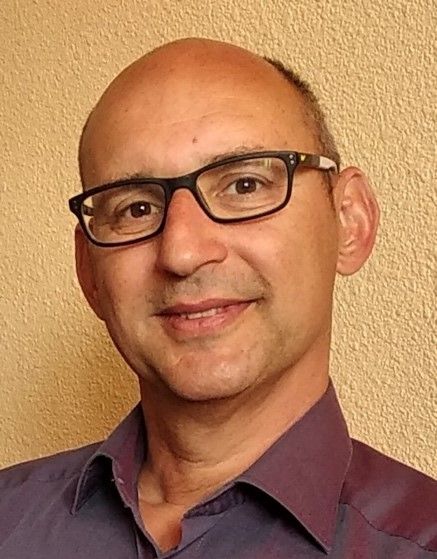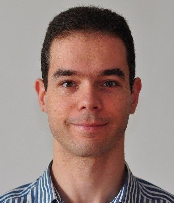
Pieter Harpe (SM'15) received the M.Sc. and Ph.D. degrees from the Eindhoven University of Technology, The Netherlands, in 2004 and 2010, respectively. In 2008, he started as researcher at Holst Centre / imec, The Netherlands. Since then, he has been working on ultra low-power wireless transceivers, with a main focus on ADC research and design. In April 2011, he joined Eindhoven University of Technology where he is currently an Associate Professor on low-power mixed-signal circuits. Dr. Harpe is analog subcommittee chair for the ESSCIRC conference and TPC member for A-SSCC. He also served as TPC member for ISSCC and AACD, was an IEEE SSCS Distinguished Lecturer and is recipient of the ISSCC 2015 Distinguished Technical Paper Award.
Keynote Speakers
Pieter Harpe
Abstract
In this talk, we will take a look at ultra low power, low area sensor interfaces. First, the SAR ADC is reviewed as the core digitizing block for these interfaces. While limited in resolution and accuracy, the SAR ADC offers advantages in terms of chip area, scalable power consumption vs frequency, as well as scalability with technology. Next, it is discussed how capacitive and resistive sensors can be connected to such an ADC while keeping the SAR ADC benefits. Various sensor interface implementations will be presented, including versatile SAR-based interfaces and temperature sensors. On top of that, analog versus digital correction strategies for circuit imperfections are reviewed and an example of a temperature sensor with analog correction for offset, gain, and distortion is given.
Chinwuba Ezekwe
Chinwuba Ezekwe's bio coming soon.
Abstract
Abstract coming soon.
Drew Hall
Dr. Hall earned a B.S. degree in computer engineering with honors from the University of Nevada, Las Vegas, in 2005, along with M.S. and Ph.D. degrees in electrical engineering from Stanford University in 2008 and 2012, respectively. He has previously held internship positions with General Electric, Bently Nevada Corporation, and National Semiconductor Corporation, where he worked on low-power, precision analog circuit design. He was a research scientist in Intel Labs from 2011 to 2013 in the Integrated Biosensors Laboratory. In 2013, he joined the Jacobs School of Engineering at the University of California, San Diego, where he is currently an associate professor in the Department of Electrical and Computer Engineering and an affiliate professor in the Department of Bioengineering.
His research interests lie at the nexus of engineering and the life sciences. Specifically, his research group works on bioelectronics, biosensors, analog circuit design, medical electronics, and sensor interfaces. Dr. Hall received the 2011 Analog Devices Outstanding Designer Award and won 1st place in the inaugural international IEEE Change the World Competition and the BME-IDEA invention competition. He received the Hellman Fellowship award in 2014, the ECE undergraduate teaching award in 2014, the prestigious NSF CAREER award in 2015, the NIH Trailblazer award in 2019, and the Best Poster award at BioCAS 2019. He is also a Tau Beta Pi fellow.
Abstract
Molecular electronics is the concept of using single molecules as functional circuit elements. This work reports the first CMOS molecular electronics chip. It is configured as a biosensor, where the primary sensor element is a single molecule “molecular wire” consisting of a ~100 GΩ, 25 nm long alpha-helical peptide integrated into a current monitoring circuit. The engineered peptide contains a central conjugation site for the attachment of various probe molecules, such as DNA, proteins, enzymes, or antibodies, which program the biosensor to detect interactions with a specific target molecule. The current through the molecular wire under a dc applied voltage. The detected signals are millisecond-scale, picoampere current pulses generated by each transient probe-target molecular interaction. Implemented in a 0.18 µm CMOS technology, 16k pixel circuits are arrayed with a 20 µm pitch and read out at a 1 kHz frame rate. The resulting biosensor chip provides direct, real-time observation of the single-molecule interaction kinetics, unlike classical biosensors that measure ensemble averages of such events. This molecular electronics chip provides a platform for putting molecular biosensing “on-chip” to bring the power of semiconductor chips to diverse applications in biological research, diagnostics, sequencing, proteomics, drug discovery, and environmental monitoring.
Timothy Denison
Professor Denison holds a joint appointment in Engineering Science and Clinical Neurosciences at Oxford, where he explores the fundamentals of physiologic closed-loop systems in collaboration with the MRC Brain Network Dynamics Unit. Tim also serves as an advisor to several governments and industry boards on the field of translational medical devices; in particular, helping define strategies for mapping scientific discovery to product development roadmaps within the regulatory and economic constraints of medical systems. Prior to Oxford, Tim was a Technical Fellow at Medtronic PLC and Vice President of Research & Core Technology for the Restorative Therapies Group, where he helped oversee the design of next generation neural interface and algorithm technologies for the treatment of chronic neurological disease. In 2015, he was elected to the College of Fellows for the American Institute of Medical and Biological Engineering (AIMBE). He has an MS and PhD from MIT in electrical engineering, and an AB in Physics and MBA from the University of Chicago.
Abstract
The total economic cost of neurological disorders exceeds £100B per annum in the UK alone, yet pharmaceutical companies continue to cut investment. The emerging field of bioelectronics suggests a novel alternative to pharmaceutical intervention by using electronic hardware to intelligently sense and stimulate the nervous system.
I will summarize the challenges and opportunities of translational bioelectronic systems face when bridging basic science, regulated technology, and health care economics. This assessment motivates an innovation framework that leverages the unique capabilities of electronic platforms -- from designing implantable scientific instruments that enable novel clinical neuroscience, to applying the resulting science to prototype new therapies.
To provide an illustrative example of the platform and innovation framework, I will highlight the “Picostim-DyNeuMo,” a collaborative, investigational research tool co-developed by UK industry (Bioinduction Ltd, Finetech Medical Ltd) and academics based on Bioinduction’s Picostim platform. The Picostim-DyNeuMo is targeting first-in-human clinical studies exploring challenging neurological disorders such as epilepsy, chronic pain, and disorders of consciousness.
Yogesh Ramadass
Yogesh Ramadass received his B. Tech. degree from IIT-Kharagpur and the S. M. and Ph.D. degrees from MIT, all in Electrical Engineering. He is currently a Distinguished Member of Technical Staff and the Senior Director of Nanotech R&D group at Kilby Labs, Texas Instruments where he is involved in research and product development efforts on MEMS, Sensors, Magnetics and Photonics. Prior to this role, Yogesh managed the power management R&D group at Kilby Labs and has held various IC design positions building products for consumer, automotive and industrial applications.
Dr. Ramadass was awarded the President of India Gold Medal in 2004, the EETimes ‘Innovator of the Year’ award in 2013 and the ‘Young Alumni Achiever’ award by IIT-Kharagpur in 2018. He was a co-recipient of best paper awards at CICC 2018 and ISSCC 2009 and the Beatrice Winner award for editorial excellence at ISSCC 2007. He is a senior member of the IEEE and has served as the chair of the ‘Power Management’ sub-committee at ISSCC from 2018-2022, as an IEEE SSCS Distinguished Lecturer from 2019-2020, as an associate editor of the IEEE Journal of Solid-State Circuits from 2015-2018 and on the Technical Program Committee for the IEEE Symposium on VLSI Circuits from 2016-2018 and IEEE ISSCC from 2013-2017.
Abstract
As sensors become ubiquitous in personal electronics, automobile and industrial settings, the need for them to do complex functions in tiny form factors is growing. The power management blocks within a sensor system play an important role not just in extending the lifespan of sensors but in making them smaller, more precise and in certain cases completely energy autonomous. This talk will go over the recent advances in materials, architectures and circuit techniques related to power management to advance the efficiency, density and accuracy of sensors.
Carolina Mora Lopez
Carolina Mora Lopez received her Ph.D. degree in Electrical Engineering in 2012 from the KU Leuven, Belgium, in collaboration with imec, Belgium. From 2012 to 2018, she worked at imec as a senior researcher and analog designer focused on interfaces for neural-sensing applications. She is currently the Scientific Director and team leader of the circuits for neural interfaces team at imec. Her research interests include analog and mixed-signal circuit design for sensor, bioelectronics and neural interfaces. Carolina is a senior IEEE member and serves on the technical program committee of the VLSI circuits symposium, ISSCC and ESSCIRC conferences.
Abstract
Abstract coming soon.
Matthias Eberlein
Matthias Eberlein received the German Diplom in Semiconductor Electronics from TU Darmstadt in 1995. He started his career with Infineon in Munich, working on cellular IPs, and later on power management topics with assignments in Germany and Asia. Recently he has been with Intel and Apple, but he is also associated with Johannes Kepler University in Linz/Austria, where he completed (in 2021) his PhD studies on thermal sensor topics.
Matthias is an IEEE senior member, authoring various publications and about 30 patents. He is recipient of the first "IEEE Brokaw Award for Circuit Elegance" in 2020. His main research interests include low-power, sensor and reference circuits in FinFET technologies.
Abstract
Thermal management becomes a demanding task in modern SoCs: In order to control and optimize computing performance, it requires tiny but smart sensors which can fit into highly constrained digital areas. Ideally those sensors can operate at low power and with a decent raw precision, since effective trimming is hardly feasible during production test. A specific challenge arises in recent FinFET technologies, where the conventional transducer – the parasitic PNP bipolar device - suffers from serious linearity issues.
This talk presents an innovative sensor concept, where PTAT and CTAT voltages are generated precisely by switched-capacitor timings. In replacement of the classical BJT, it utilizes the active bulk diode of a standard CMOS process and provides forward biasing by a charge-pump. During the periodic capacitor discharge the respective pn-junction voltages are sampled at different time points and evaluated by passive charge-balancing.
The architecture features intrinsic supply robustness down to ~0.85V and enables temperature sensing at low circuit complexity: A prototype with a simple 8-bit capacitive SAR scheme occupied 2500 μm2 silicon area in 16nm FinFET. Thanks to the superior linearity of the bulk diode, it achieved an accuracy of ± 2°C without trimming across several wafer lots. Due to the pulse width control and low analog content, this concept is suitable for hotspot sensing and insensitive to future scaling.
Tim Piessens
Tim Piessens received the M.Sc. and Ph.D. degrees in electrical engineering from the Katholieke Universiteit Leuven, Leuven, Belgium, in 1998 and 2003, respectively. During his Ph.D., he focused on a new type of power amplifier/line driver for xDSL applications. In 2004, he co-founded Icsense, where he was the CTO and was responsible for the technical content of projects in the medical, automotive and consumer fields. His current research interests include analog sensor readouts, non-linear system design, power management, high-voltage design and low-power, low-noise analog front-end design. From 2014 till 2021, he was a member of the IEEE International Solid-State Circuits Conference Technical Program Committee. He was a member of the ISSCC EU leadership, the ISSCC executive committee and the ISSCC vision committee from 2019 till 2021 and ITPC EU chair in 2021. From 2020 on, he is a member of the ESSDERC-ESSCIRC Steering Committee.
Abstract
Barometric pressure sensor are indispensable features in wearable consumer devices. Modern designs can sense absolute height difference of less than 8.5cm (1Pa), improving indoor navigation significantly and enabling new applications such as activity tracking and crash detection. In this talk, we will take a deep dive into the design challenges of readout chains for capacitive pressure sensors developed at TDK. The main driving requirements are noise and power. To reach the demanding targets for wearable devices, heavy duty cycling and advanced analog front-end design is needed. But these are not the only challenges. Since they must be exposed to the atmosphere, pressure sensors in smartphones are often located in their outer cases, and have long connections to the main PCB. This leads to high demands on their PSRR and RF immunity. Both topics will be discussed, as well as several methods to improve the robustness of pressure sensor readout chains.